Nano Photonics
Monolithic plasmonic circuits
Guided wave plasmonic circuits hold promise for various applications such as sensing, interconnection, and quantum functionalities in the sub diffraction regime. However, a significant challenge in these circuits is the loss confinement trade-off, limiting their efficiency. Therefore, plasmonic-based processes based on an amorphous material have been used to address this challenge and enhance device efficiency.
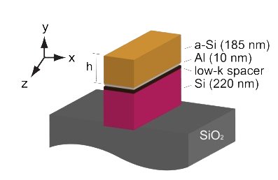
Schematic of the multilayer CHPW structure
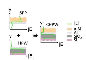
Supermode engineered through coupling of SSP and HPW modes
By fabricating device which offer integration of both passive and active optical components on a single substrate utilizing surface plasmons record promising experimental results. These attributes include a normalized Purcell factor approaching 104, 10 dB amplitude modulation with less than1 dB insertion loss and switching energy at the femtojoule level. The structure also exhibits high photodetection sensitivity, with a reported value of -54 dBm, along with an internal quantum efficiency of 6.4%. This has been realized within our amorphous-based, coupled-mode plasmonic structure.
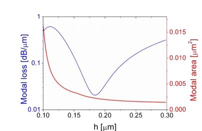
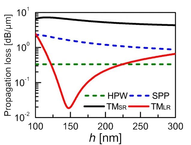
Calculated modal area and propagation loss
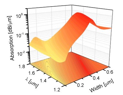
Supermode as a function of waveguide width and operation wavelength
Thus, plasmonic waveguide design not only alleviates the plasmonic loss-confinement trade-off but can utilize multiple device physics to enable multiple functionalities. Based on a unique class of asymmetrically coupled supermode, our amorphous-based devices demonstrated record Purcell factor for plasmonic microrings, record quantum efficiency and sensitivity for guided-wave Schottky detectors, as well as record extinction ratio insertion loss (ER-IL) for plasmonic modulators based on epsilon-near-zero (ENZ) effect.
Amplitude modulation using ENZ effect
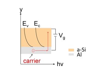
Photodetection based on internal photoemission at the
Schottky interface
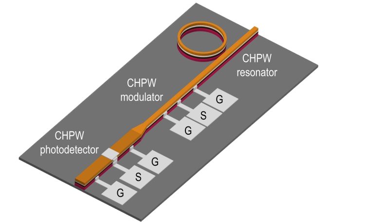
Vision of monolithic plasmonic circuitry
Furthermore, CHPW platform offers versatility, as resonators and photodetectors can also be realized within the modulator stack by adjusting the carrier density of ITO and utilizing IPE at the ITO-Si Schottky junction, respectively. In conclusion, the flexibility of the CHPW platform allows for the implementation of identical waveguide elements that can be electrically reconfigured to support different passive and active functionalities.
https://DOI: 10.1021/acs.nanolett.9b04612
Purcell factor
Ohmic loss is the major issue particularly in coupled hybrid plasmonic waveguides (CHPW) ring resonators. This loss hinders the practical use of superior wave-matter interaction offered by plasmonic, especially as mode volume is reduced. To solve the limitations posed by ohmic losses in integrated optical devices and traveling-wave resonators composite hybrid plasmonic waveguides (CHPWs) based on dissimilar plasmonic modes are introduced. These waveguides can guide subwavelength optical modes with long-range propagation while versatile in fabrication and design.
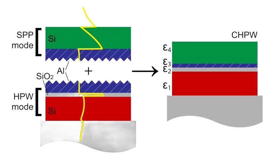
CHPW structure formed by coupling of SPP and HPW
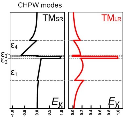
The coupling gives rise to transverse magnetic short-range (TMSR) and long-range (TMLR) supermodes
However, In the context of ultracompact hybrid plasmonic ring resonators Purcell factors can be significant due to the strong confinement of electromagnetic fields within the plasmonic structures. But, specific values of Purcell factors in such resonators can vary widely depending on the exact design parameters, materials used, and operating conditions. Obtaining precise Purcell factor values typically requires sophisticated theoretical modeling and experimental characterization.
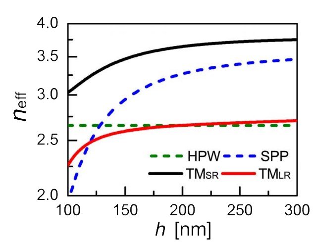
Effective mode index
SPP and HPW modes are plotted for comparison
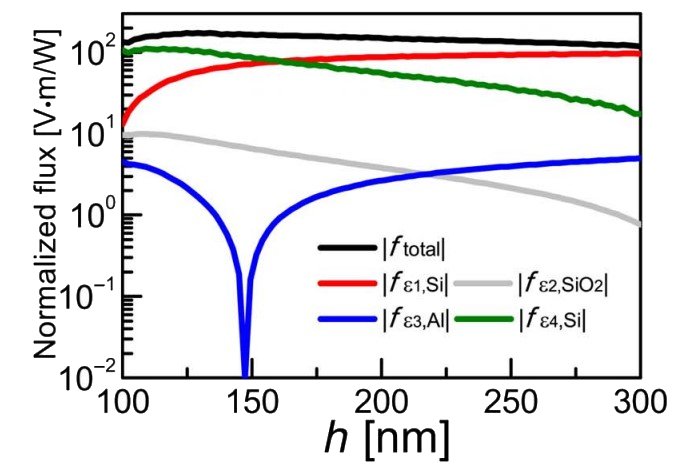
Experimental investigation realized that the propagation loss and modal area of 0.03 dB/mm and 0.002 µm2 corresponds to the smallest combination among long-range plasmonic structures. It can also demonstrate that the CPHW ring resonators with 2.5-µm radius with a record Purcell factor, surpassing the performance of existing plasmonic and dielectric resonators of similar radii. Through this combination, 6507 normalized Purcell factor can be achieved as the adverse effect of the ohmic loss inherent to plasmonic is drastically alleviated using our structure.
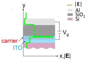
The normalized 1D field profile of CHPW
The modal loss can be decreased by two orders
of magnitude while modal area is relatively invariant
Moreover, the experimental demonstration of CHPW microring resonators with high Purcell factor utilized for Nanolaser, Cavity Quantum Electrodynamics (QED), Nonlinear Plasmonics, Photodetection Efficiency Optimization, Integrated Optical Circuitry applications. These potential applications underscore the versatility and promise of CHPW microring resonators, indicating their relevance across various fields within photonics and nanotechnology.
https://DOI: 10.1126/sciadv.aav1790